Blog
The Upside Down: The Bottom-side Envelope of the Compute Node PCB
Introduction
OpenSFF is a nonprofit organization developing a set of open-source hardware specifications. Our documents define three components: a processing module called the Compute Node, an active electronic housing for one or more nodes called the Enclosure, and an optional node management device called the Management Module.
Those three components can be combined to create a wide number of vendor-agnostic systems, from servers to edge devices. As such, we are making sure that vendors have sufficient flexibility to tailor their implementations for their intended use case or audience. That includes the component selection and layout for Compute Nodes.
The Compute Node Specification explicitly states that the underside of the node’s PCB has a 6mm height envelope. While that may not sound like a lot of space, in this article we are going to explore how there are actually many components that fit within that envelope.
What the Compute Node Specification says
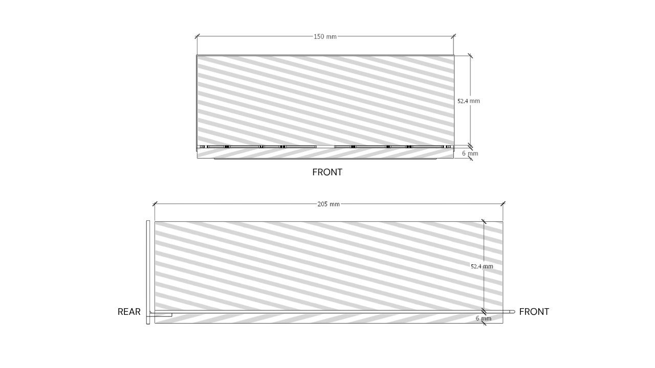
The Compute Node PCB is 205mm long x 150mm wide x 1.5mm thick. Note that the usable board area will be smaller than what those measurements imply, because we define keepouts for features such as the guide rail and the retention points for the I/O shield. As for the height clearances, the top-side envelope is 52.4 mm while the bottom-side envelope is 6mm, as previously mentioned.
While we could have lowered the board by a few millimeters more, we believe that 52.4mm is enough, considering that most of that height will be used by passive cooling solutions, and Compute Nodes have a 120W maximum power target (MPT).
With our measurements defined, let us go over how vendors can maximize the underside of the Compute Node’s PCB.
What vendors can add on the underside of the PCB
Storage
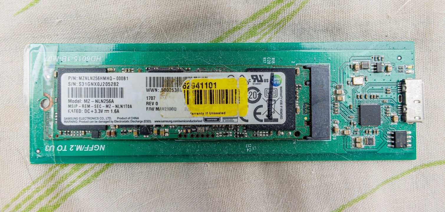
M.2 storage will likely be one of the most common occupants of the board’s underside space. Single-sided modules are only 2mm tall, while double-sided ones are 3mm. Our bottom-side envelope gives vendors enough height for a double-sided M.2 SSD along with a low-profile heat spreader. This layout is already widely used in mini PCs and NAS devices.
Vendors can of course explore other forms of storage to place on the bottom of the node PCB, including a microSD card slot, which is only about 2mm tall. A microSD card can serve as a storage for OS or firmware images, a read-only boot partition, or a recovery target.
Memory, networking, and additional compute
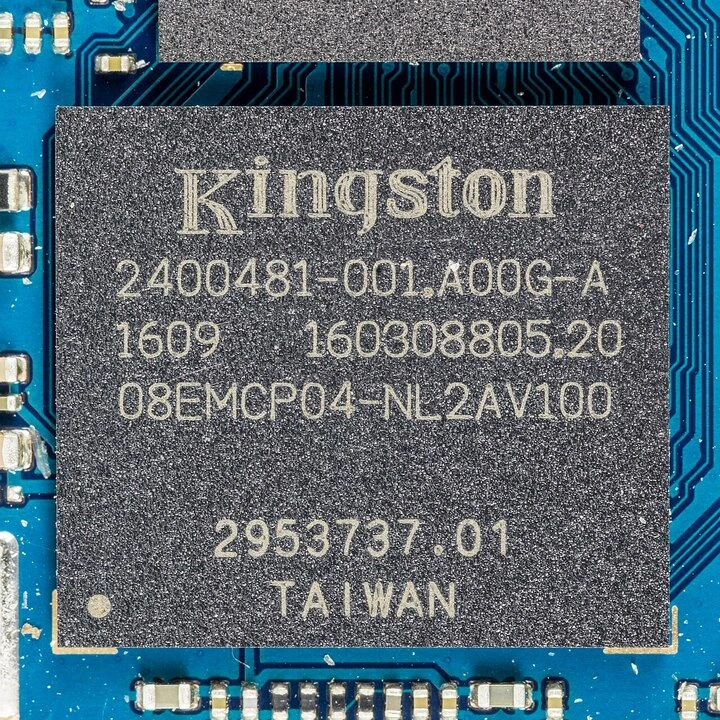
Similar to M.2 storage, soldered memory and eMMC are also commonly mounted on the PCB underside, especially in SoCs and SoMs/CoMs. Network controllers are another type of essential system component that should easily fit under a Compute Node’s PCB. For instance, the Intel I225/I226 NICs are only 0.86mm tall.
Board support
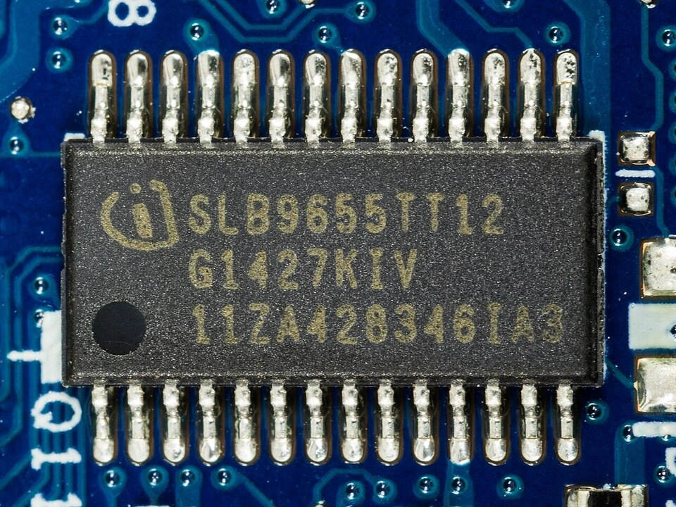
A variety of supporting components can also easily fit on the bottom-side of the node PCB. A discrete TPM chip is about as tall as a NIC. There are also PMICs and DC-DC converters that easily fit in our extra space. For instance, Analog Devices explicitly markets the low-profile of its LTM4622 regulator as an advantage, allowing the component to be mounted on a PCB’s backside. An RTC coin-cell paired with a low-profile holder can also fit under a Compute Node’s PCB.
Expansion
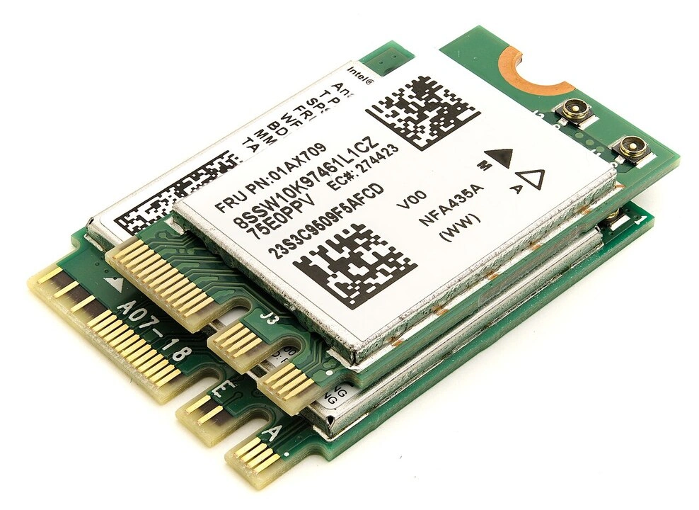
Besides storage modules, there are other components that can be slotted into an underside-mounted M.2 slot, such as Wi-Fi, Bluetooth, and cellular modem cards. There are also more specialized cards such as ones that provide serial connectivity, or cards that offer 24 channels of digital I/O. An underside-mounted M.2 slot can be adapted into the various use cases for which our standard is designed, such as edge, embedded, and industrial.
Considerations for bottom-side PCB components
This being a common practice, many board makers and device manufacturers have documented the tradeoffs of double-sided PCBs. Some bottom-side components require a second reflow soldering pass, a process that adds cost and risk of failure. The overhead varies with the components and how they are mounted on the board.
When it comes to manufacturing failures, components can fall when the board is flipped for the second reflow pass. The solder on the reflowed side can melt again, which may then cause relatively heavy components to detach.
Thermal stress is also a concern for double-sided boards. Doubling the thermal cycle can lead to warpage or weak solder joints.
The extra soldering process and the risks associated with it necessitate additional or more rigorous inspection. If there are hidden solder joints such as BGAs after the reflow process, 2.5D or 3D X-ray inspection may be needed to check the assembly’s quality.
Build with OpenSFF
We define the bottom-side PCB envelope as intentional headroom for vendors, making Compute Nodes considerably more spacious than its top-side dimensions suggest. Given our 120W node MPT, adding more height top-side is unnecessary. Leaving 6mm for the board’s underside provides plenty of space for standoffs or backplates. More importantly, it gives vendors the option to relocate components off of the top-side.
Components such as M.2 storage, network controllers, and low-profile board supports are already commonly mounted on the underside of PCBs in many other devices. Vendors who wish to test the limits of the node’s underside volume can look into larger components such as double-stacked M.2, larger NAND packages, or perhaps PCIe 3.0 x2 accelerator cards.
We encourage you to read our specifications, and we would be grateful if you spread the word about OpenSFF. For technical clarifications, partnerships, and other inquiries, reach out to our development team at [email protected].
Other Articles

Meet OpenSFF: an open hardware standard that enables cross-vendor compatibility, modular systems, and sustainable hardware reuse.
August 11, 2025
We go over the rise of virtualization and the open software adopted by home server enthusiasts, as well as the current challenges and the future of the hobby.
September 06, 2025

Learn why OpenSFF adopted the SFF-TA-1002 connector standard and how it enables our vision.
September 18, 2025