OpenSFF Compute Node Specification
Download as PDF3. Physical Characteristics
This section details the physical characteristics and mechanical specifications for the compute node. Adherence to these guidelines ensures proper fit, function, and compatibility within the OpenSFF ecosystem.
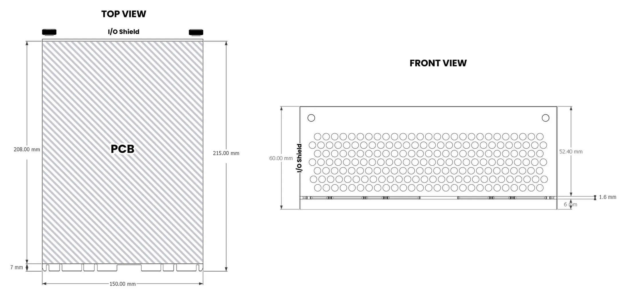
3.1 Overall Compute Node Dimensions
The compute node MUST conform to the following overall dimensions, including the cooling shroud and I/O shield:
| Parameter | Value | Notes |
|---|---|---|
| Length | 215 mm | Measured from the inside mating surface of the I/O shield to the end of the connector plug |
| Width | 150 mm | Full width of the I/O shield |
| Height (Total) | 60 mm | Includes PCB, components, and cooling shroud |
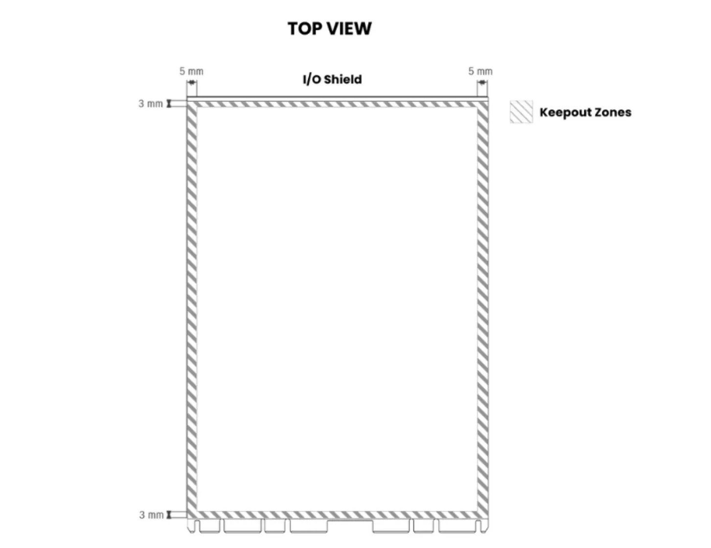
3.2 Component Placement and Keep-Out Zones
This section defines the permissible dimensions for components on the PCB and areas where components MUST NOT be placed.
3.2.1 Top Components
The top side of the compute node PCB is typically populated with the following components:
- CPU and thermal solution
- Memory (SODIMM/CAMM/on-board)
- Voltage Regulator Modules (VRMs) and chokes
- M.2 slots and NVMe drives
- Other Surface Mount Devices (SMDs)
Maximum Dimensions for Components on the Top Side of the PCB:
- Length: 202 mm (centered): Maximum usable length, excluding the physical Core/Enterprise connector plug, accounting for keep-out zones along the PCB edges facing the edge plug and the I/O shield.
- Width: 140 mm (centered): Maximum usable width, allowing clearance for the PCB card support guides (see Section 3.5) and the air shroud (see Section 6.3).
- Height: 50 mm: Maximum height, considering PCB thickness and internal shroud height (see Section 6.3).
3.2.2 Bottom Components
The underside of the compute node PCB is typically populated with the following components:
- Thermal solution backplates
- M.2 slots and drives
- Other Surface Mount Devices (SMDs)
The maximum dimensions of the components under the PCB MUST NOT exceed:
- Length: 202 mm (centered): Maximum usable length, excluding the physical Core/Enterprise connector plug, accounting for keep-out zones along the PCB edges facing the edge plug and the I/O shield.
- Width: 142 mm (centered): Maximum usable width, allowing clearance for the PCB card support guides
- Height: 6 mm
Components requiring consistent active or robust passive cooling (e.g., high-performance NVMe SSDs) are generally NOT recommended for placement on the bottom of the PCB due to limited airflow. Designers must ensure adequate thermal management for any heat-generating components in this area.
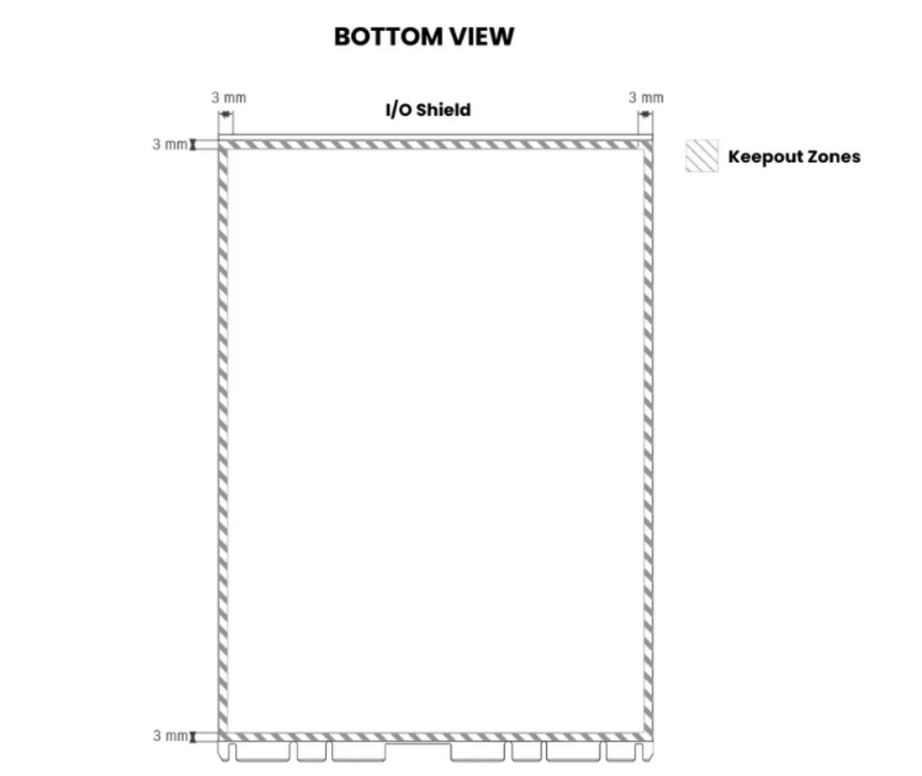
3.2.3 General Component Placement Restrictions
Component placement on both the top and bottom of the PCB MUST be restricted in the following areas:
- Length: To accommodate keep-out zones from the I/O shield and edge plug.
- Width: To allow space for the PCB card support guides and the node’s air shroud (top side only)
- Height: To allow easy insertion and removal and avoid interference with other enclosure components.
3.3 I/O Shield
The compute node MUST include a metal I/O shield to act as physical protection, airflow egress, electromagnetic interference (EMI) shielding, access to optional external connectors, and a mounting solution.
The I/O shield MUST have the following dimensions:
- Width: 150 mm
- Height: 60 mm
- Thickness: 1.2 mm (minimum)
The I/O shield MUST be perforated, to act as an exhaust for the node's cooling system.
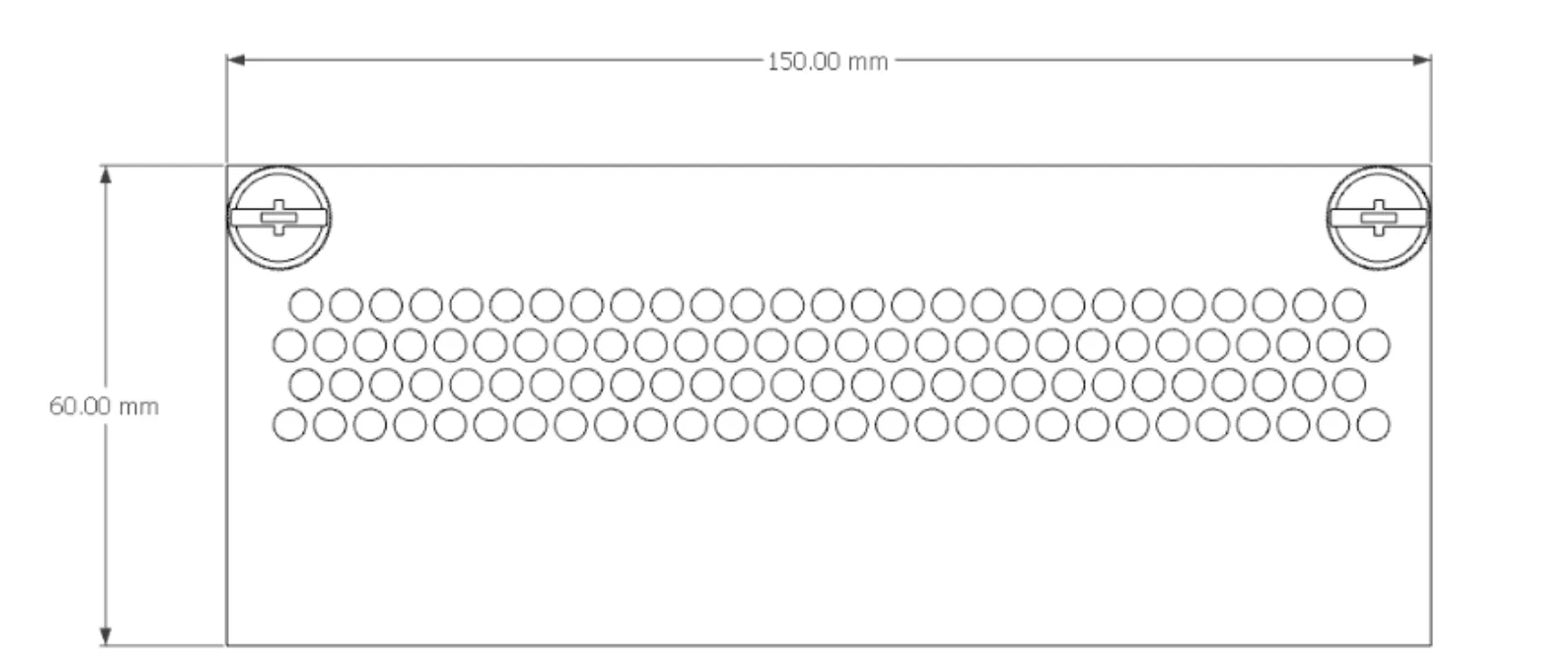
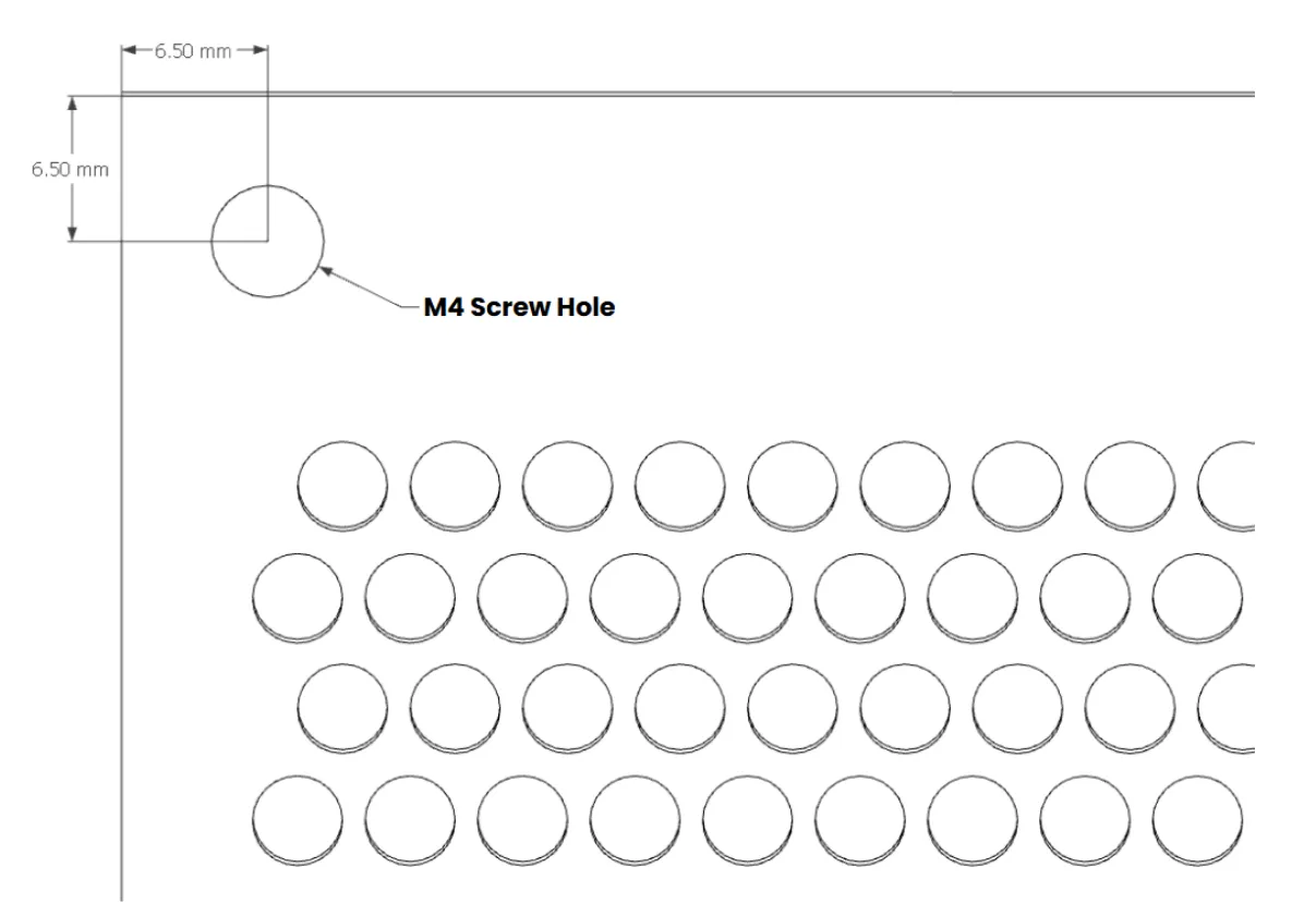
The I/O shield MUST be mounted using two captive M4 thumbscrews and matching screw holes, with the following specifications: /
- Mounting: Two captive M4 thumbscrews.
- Hole Center Location: 6.5 mm from top and side edges of the I/O shield.
- Screw Hole Clearance: Minimum 2.5 mm clearance around the screw hole (measured at the inside mating surface of the I/O shield).
Additional connectors on the I/O shield may be connected at the manufacturer's discretion.
3.4 Mechanical Envelope and Retention Interface
OpenSFF compute nodes are designed for blind-mate insertion into compatible enclosure slots. This section defines the required mechanical envelope, rear connector alignment, and retention mechanism to ensure consistent fit and serviceability across OpenSFF enclosures.
3.4.1 Connector Alignment Plane
The compute node’s connectors are designed for blind-mate insertion into an enclosure-defined node bay envelope, which establishes the physical reference for connector positioning.
Connector alignment MUST comply with the following:
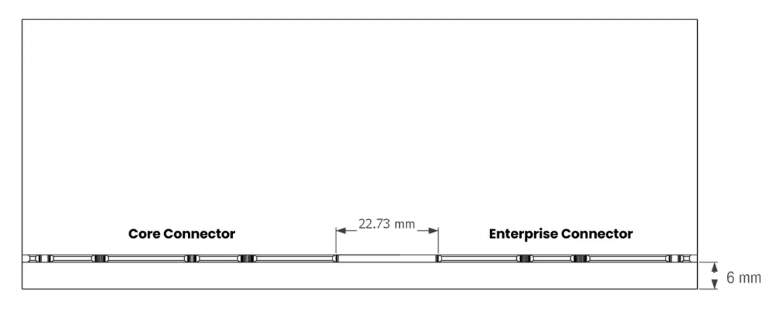
- The Core connector (4C+) MUST be positioned such that its outermost guide notch is exactly at the right edge of the I/O shield envelope (as viewed from the rear)
- If present, the Enterprise connector (4C) MUST be positioned such that its outermost guide notch is exactly at the left edge of the I/O shield envelope
- The horizontal distance between the inner faces of the two connectors (excluding guide notches) MUST be 22.73 mm
- Both connectors MUST be co-planar for reliable blind-mate insertion
3.4.2 Enclosure Retention Interface
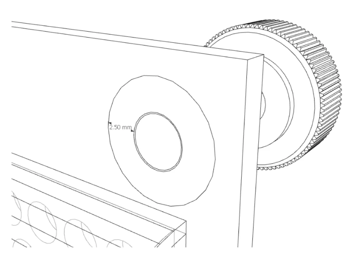
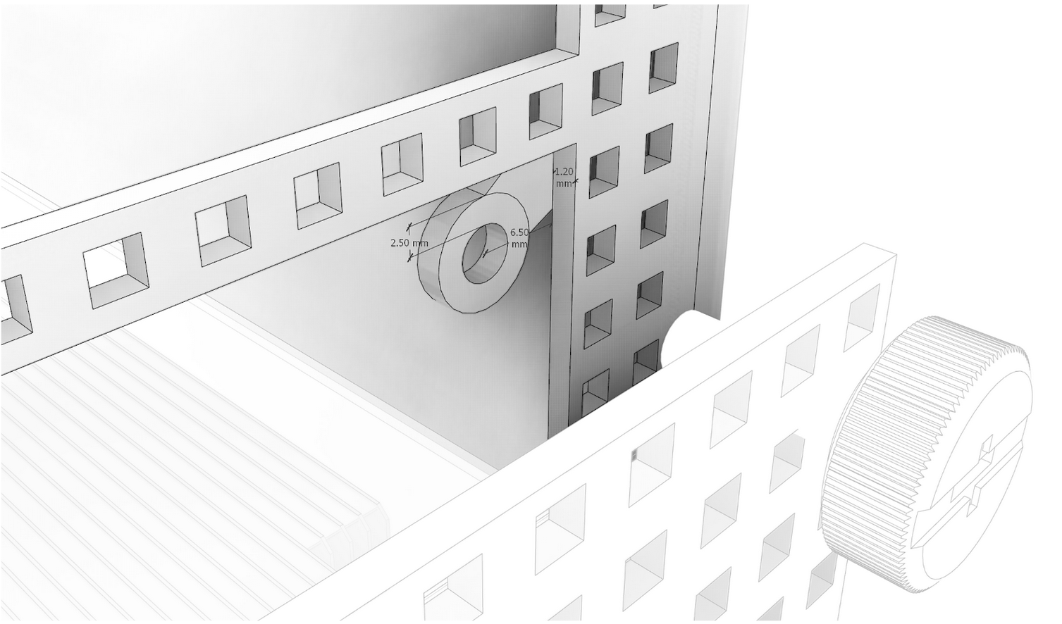
The compute node is secured within the enclosure using two captive M4 thumbscrews integrated into its rear I/O shield, as specified in Section 3.3. The enclosure MUST provide compatible threaded mounting points that align with the screw hole positions and support tool-less installation.
Specifically, the enclosure MUST:
- Position threaded retention points to match the node’s 6.5 mm offset from the top and side edges of the I/O shield
- Provide a rigid backing structure to prevent flex during tightening or vibration during operation
- Maintain a 2.5 mm clearance radius around each mounting point to avoid interference with the cooling shroud
- Recess the screw mating surface by 1.2 mm from the enclosure's interior panel face to accommodate the I/O shield thickness and ensure flush contact during retention
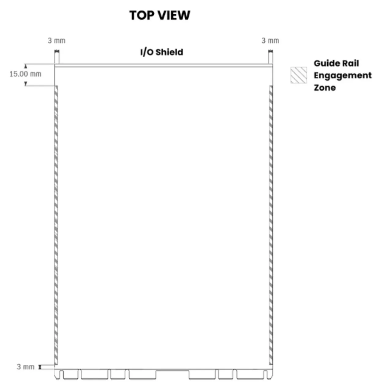
3.5 PCB Guide Rail System
To ensure proper alignment, reduce connector wear, and support vibration and shock mitigation, compute nodes MUST accommodate enclosure-based PCB guide rails. This section defines the required interface clearances and alignment zones for compute node PCBs intended to operate such systems.
Specifications:
- The compute node PCB MUST reserve space for engagement with a dual vertical guide rail system provided by the enclosure.
- Two vertical guide rails SHALL be positioned parallel to the compute node’s length axis, along the left and right edges of the PCB.
- The guide rails SHALL extend from the rear edge of the node (opposite the I/O shield) and MUST terminate no closer than 15 mm from the front face of the I/O shield.
- A minimum clearance zone of 3 mm MUST be maintained between the outer edge of the PCB and each guide rail (both sides).
3.6 Temperature and Humidity Requirements
The compute node MUST be designed to operate within the following temperature and humidity ranges:
- Operating temperature: 10 °C to 35 °C
- Storage temperature: –40 °C to 65 °C
- Relative humidity: 8% to 80% (non-condensing)
3.7 Vibration Resistance
The compute node MUST be designed to withstand vibration levels encountered in typical operating environments. See section 7.3.1 for testing specifications.
3.8 Environmental Tolerance
Compute nodes MUST operate reliably in environments with typical indoor air quality, including the presence of fine dust or particulate matter (PM5 or smaller), consistent with ISO 14644-1 Class 9 cleanliness levels. Nodes are NOT required to meet a formal Ingress Protection (IP) dust rating; however, they must exhibit baseline environmental resilience by withstanding standardized particulate exposure and durability validation tests. Designs SHALL NOT rely on user-replaceable air filters within the compute node itself to maintain operational integrity under these conditions.
Design considerations for dust resilience:
- All components critical to system operation (including CPU sockets, memory modules, VRMs, and the like) must be positioned to limit direct accumulation of non-conductive dust
- The shroud and its airflow pathways should be designed to reduce turbulence and stagnation zones where debris can accumulate
- Where feasible, PCB coatings MAY be used to mitigate the effects of inductive or corrosive dust ingress
Serviceability Guidelines:
- Compute nodes must be field-serviceable using non-specialized tools, with no requirement for internal cleaning during the expected lifecycle or warranty period (defined by vendor/manufacturing partner, not less than 3 years).
- Accessible areas (e.g. DIMM slots, M.2 storage slots) must remain free of obstructive debris that could impact upgrade or maintenance operations.
See section 7.2.7 for the testing requirements for dust/debris ingress.